


At the nanoscale frontier of semiconductor manufacturing, one of the most persistent and perplexing adversaries is not a defect or a design flaw. It is randomness itself. As transistor dimensions approach atomic scales, even the tiniest fluctuations in chemical behavior can cause significant variation in device performance. This stochastic variability, driven by probabilistic chemical events during lithography and etching, is now one of the major challenges facing chipmakers. Erik Hosler, a strategist who connects material science with multi-sector technological advancement, points out that solving this issue can require more than isolated fixes.
Controlling randomness may sound like a contradiction, but that is exactly what researchers and engineers are trying to achieve. Variations in photon counts, chemical concentrations, and reaction conditions now play an outsized role in determining yield and reliability. These are not anomalies. They are statistically expected fluctuations. As the industry continues to push below 5nm nodes, understanding and minimizing these stochastic effects is becoming essential to maintaining manufacturing precision.
The Nature of Stochastic Variability
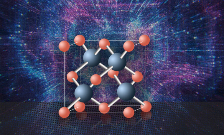
In semiconductor fabrication, stochastic effects refer to unpredictable variations that occur during processes such as photoresist exposure, post-exposure bake, and development. At extremely small scales, molecular-level events can no longer be averaged out. Each interaction matters.
For instance, during EUV lithography, photon shot noise can cause various parts of a wafer to receive slightly different energy doses. It can lead to uneven resist exposure, which in turn causes edge roughness or critical dimension variability. In some cases, entire features may fail to develop or etch properly.
Similarly, in chemically amplified resists, acid diffusion and reaction kinetics introduce randomness that affects line width control. These variations are not necessarily due to equipment error or process drift. They arise from fundamental physical limits.
Why Randomness Matters More Than Ever
As the industry pushes for denser, more powerful chips, design tolerances are shrinking. What used to be minor fluctuations are now significant risk factors. A line that is one nanometer too wide or narrow can alter the electrical behavior of a transistor, and a missing contact can shorten an entire circuit.
These inconsistencies directly impact yield. Variability leads to increased defectivity, which reduces the number of functional chips per wafer. It has economic consequences, especially as advanced process nodes become more expensive to operate.
In the past, larger design margins might have hidden such randomness. Today, those margins are gone. To maintain progress, stochastic effects must be addressed directly rather than tolerated as unavoidable background noise.
Cross-Disciplinary Strategies for Control
Taming randomness requires cooperation across the entire semiconductor ecosystem. Engineers are exploring solutions in chemistry, physics, materials, and computation. Erik Hosler mentions, “It’s going to involve innovation across multiple different sectors.”
One strategy involves designing new photoresists with more uniform molecular structures. These materials are less prone to uneven reactions, allowing for tighter process windows. Researchers are also working on resists that generate stronger signals with fewer photons, reducing shot noise.
At the same time, optical engineers are developing exposure systems with more consistent energy delivery. High-NA EUV tools, for example, offer greater resolution but require novel approaches to resist sensitivity and focus control.
Statistical modeling and machine learning are increasingly important. By simulating hundreds or thousands of process runs, engineers can identify conditions that are more likely to yield consistent results. These insights feed into process control algorithms that adapt in real time during fabrication.
Advanced Metrology and Feedback Loops
Another area of focus is detecting stochastic defects before they cause failures. Traditional inspection tools often miss the sub-nanometer variations that define stochastic events. New metrology techniques, including hyperspectral imaging and scanning probe microscopy, are being used to capture a more detailed picture of wafer surfaces.
This data is then fed into feedback loops that adjust process parameters on the fly. For example, if one region of a wafer shows signs of overexposure, the system can reduce intensity in that area for the next run. Over time, this adaptive control helps reduce the variance caused by stochastic effects.
Process analytics also helps identify subtle patterns. While the events are random, their probability distributions can be understood and influenced. It allows engineers to shift the odds in their favor, creating conditions where desirable outcomes are more likely.
Implications for Chip Design
Addressing stochastic variation does not stop at the fabrication level. It also influences how chips are designed. Engineers are now incorporating variability-aware models into their design tools, accounting for stochastic behavior during layout and simulation.
That means developing structures that are more tolerant to process variation or including redundancy in critical paths. It also requires collaboration between design and process teams to ensure that layouts align with the realities of modern manufacturing.
In advanced packaging and 3D integration, where features are stacked vertically and margins are tighter than ever, understanding how randomness propagates through layers is becoming vital. A small variation at one level can cascade into larger issues later in the stack.
Toward Probabilistic Precision
While stochastic effects can never be eliminated, they can be managed. The goal is not to create a deterministic process, but a probabilistically stable one. In this context, “control” means reducing the spread of outcomes and increasing the likelihood of success.
This probabilistic mindset is reshaping how fabs operate. Quality is no longer measured just by averages, but by variance. The industry is learning to optimize consistency, not just capability. Progress in this area can also influence how chipmakers evaluate tools, materials, and partners. The ability to work across silos, share data, and coordinate development can define the winners in the post-Moore era.
Order Within Chaos
The effort to manage stochastic variation reveals something fundamental about the future of chipmaking. It is no longer a game of raw power or single-process optimization. It is a game of orchestration, of aligning chemistry, engineering, and computation to work together in real time.
By acknowledging the presence of randomness and designing processes that account for it, the semiconductor industry is not conceding defeat. It is moving toward a more sophisticated, adaptive model of innovation.
Through shared knowledge and cross-sector collaboration, even randomness can be brought into alignment. And in that alignment lies the next generation of computing performance, delivered with precision, one probabilistic pattern at a time.


